MCU Proto Board with 3.3 and 5V Power
$9.95
Proto module with flexible 3.3 and 5V power distribution.
11 in stock
Description
This quality proto board accommodates virtually any DIP style MCU module and provides 3.3V and 5V power and power distribution.
PACKAGE INCLUDES:
- MCU Proto Board with 3.3 and 5V Power
KEY FEATURES OF MCU PROTO BOARD WITH 3.3 AND 5V POWER:
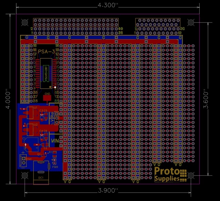
- Extra wide MCU slot that accommodates virtually any DIP style MCU Module
- Ideal for 3.3V MCUs that take 5V VIN input
- Reverse input power protection
- 3.3V and 5V LDO linear regulators
- Fully distributed power and ground with clear silkscreen top and bottom
- SOIC-28 and TSSOP-28 footprints
- Standard 0.1″ / 2.54mm hole patterns with extra large plated through holes and pads
- High quality construction with ENIG (Electroless Nickel Immersion Gold) finish
- Compact 4.3″ x 4″ size
These boards are a great option when it comes time to move a small to medium size MCU project from the solderless breadboard to a more permanent construction. This board is similar to our MCU Proto Board with DC Input, but this version includes both 3.3V and 5V LDO regulators to power the microcontroller and/or power rails and comes fully assembled.
These are especially handy for 3.3V MCUs designed to operate from 5V like the Teensy products. The 5V can be used to drive the VIN input of the MCU while the 3.3V can power the power rail. They also work well with MCUs that take a higher voltage on their VIN input where VIN on the board can connect to the VIN input of the MCU and the power rail can operate at 3.3V or 5V as needed.
Compatible with Wide Variety of MCUs
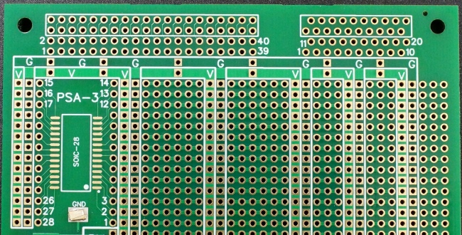
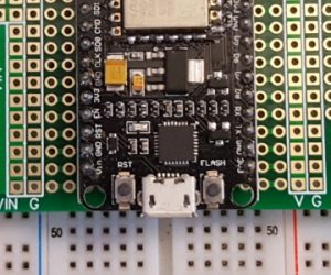 This board incorporates an extra wide center section to facilitate mounting virtually any DIP style MCU from very narrow to very wide.
It features a standard 0.3″ wide center with power and ground rails. Extra wide 6-hole pad pattern on either side makes it wider than a standard solderless breadboard. The MCU section is 32 pins long.
This configuration allows the board to be used with anything from as small as a Attiny85 DIP IC to the sometimes too wide ESP8266 NodeMCU or the extra long Teensy 4.1. It will also fit any of the Arduino DIP style modules like the Nano or Micro.
This section can also be handy for mounting other wider pinned modules such as some types of LED driver modules.
Flexible Power Options
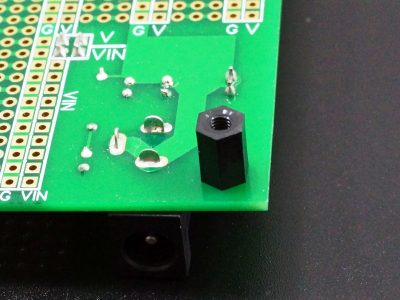
The input section of the board provides for multiple power options.
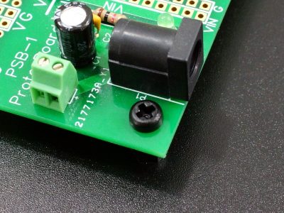
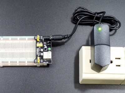
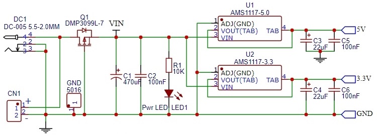
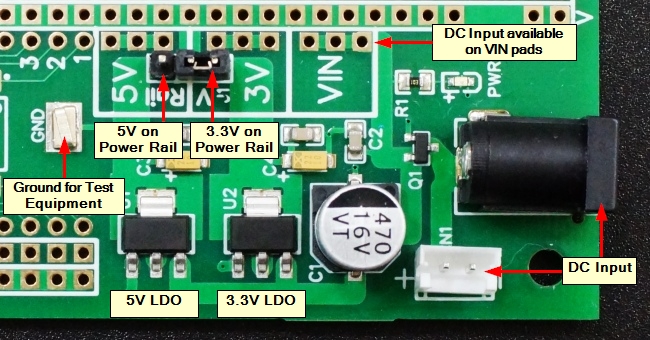
Power can be connected via a standard DC power jack or a JST PH-2.54 style 2-pin battery connector. The input voltage can be between 6-14V. 6.3 to 9V is recommended.
This VIN input section has MOSFET reverse power protection, filter capacitors and a green power on LED. This VIN input power is available on several marked pads for easy jumping to the VIN input of an MCU that needs to be powered off this higher raw input voltage such as a Nano.
The VIN input powers both a 3.3V and 5V AMS1117 LDO regulator with filter capacitors on their outputs. The 5V regulator is guaranteed to operate down to 6.3V, but under lighter loads will regulate down to 6V. Since they are linear regulators, they benefit from having the lowest possible input voltage to minimize power dissipation when used for higher current loads.
The LDOs are mainly suited for providing good clean power for peripherals, to offload this requirement from the MCU on-board LDO regulators or to feed the MCU on-board 5V to 3.3V LDO regulator. If more current is required a small DC-DC converter module can be installed on the board and fed from the VIN input. The reverse power protection MOSFET is rated for a maximum of 3.8A.
Flexible Power and Ground Distribution
There is a jumper block so that either the 3.3V or 5V LDO output can be connected to the power rail labeled ‘V‘ on the board. The ground rails are labeled ‘G‘.
All power and ground runs are silk-screened on both sides of the board and the VIN and V power rails and ground pads are square to further clearly differentiate them.
The distributed power and ground runs allow for easy placement of additional bypass or filter caps as needed if the board mounts high speed / high current circuits.
There is a handy ground clip located at the top of the power section for connecting the ground of a O’scope or other probe.
Flexible Prototype Areas
Besides the wide MCU area, the board also has an SOIC-28 0.3″ wide footprint with 0.050″ lead pitch on top and a mirrored TSSOP-28 footprint with 0.025″ lead pitch on the bottom. These can be used to mount one large or a couple of smaller SMD ICs. The pins are brought out to numbered solder pads. If using with ICs smaller than 28-pins, the pin number will need to be adjusted.
The rest of the prototyping area uses a 3-hole pad pattern to keep things compact.
The back edge of the board has a 2 x 20 header area with separate solder pads as well as a 2 x 10 area with offset pads that can be useful for some types of connectors that use offset pins such as RJ45s.
All holes are large 40 mil plated through with large 70 mil pads. These are large enough to use with TO-220 type packages like power MOSFETs.
The 3-hole and 6-hole patterns have 30 mil traces connecting them for good current handling capability. Power and ground runs are 80 mil.
High Quality Finish
The boards are constructed of 1.6mm FR-4 with 1oz copper.
The copper has an ENIG (Electroless Nickel Immersion Gold) finish for maximum performance. ENIG ensures extended shelf life against corrosion, provides excellent solderability with lead or lead-free solder, provides a completely flat soldering surface and gives good visibility of the soldered joints compared to the gold plating. It is also fully ROHS compliant.
Green solder mask is used as it provides the highest performance compared to other colors and also provides excellent trace visibility in case trace customization is desired.
Input Power Considerations
The DC input voltage directly affects the maximum amount of current that can be drawn from the LDO regulators since they have to drop the excess voltage as heat. The higher the input voltage, the less current that will be available.
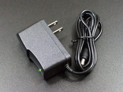
For that reason our 7.5V AC/DC adapter is a good match for this board. With a 7.5V input, the 5V LDO can support up to 750mA and the 3.3V LDO can support up to 400mA.
If the input is operated at the guaranteed minimum of 6.3V, the 5V LDO can reach close to the full 1A output and the 3.3V LDO can output about 440mA.
If you only care about 3.3V, you can power the board off 5V and pull close to the full 1A off the 3.3V LDO. In that case, the 5V LDO output would not be usable but the 5V input would be available on the VIN pads.
At higher input voltages and currents, the LDOs can get quite hot, so use care when touching them. The LDOs do have automatic thermal shutdown and other protections, so they will typically shutdown safely if overloaded or outputs are shorted to ground.
Board Mounting
The board is 4.3 x 4″. It has four 0.138″ diameter holes which can accept up to 3.5mm or #6 screws. The holes are spaced 3.9 x 3.6″ apart.
Notes:
- None
Technical Specifications
| Material | FR-4 | |
| Copper | 1 oz, double-sided | |
| Plating | ENIG (Electroless Nickel Immersion Gold) | |
| Solder Resist | Green | |
| Silkscreen | Front and Back | White |
| Prototype Area | Holes, plated-thru | 1.02mm (0.04″) |
| Pads | 1.78mm (0.07″) | |
| Dimensions | Board outline | 109.2 x 101.6mm (4.3x 4.0″) |
| Board thickness | 1.6mm (0.062″) | |
| Mounting holes | 3.5mm (0.138″) | |
| Mounting holes center-center | 99 x 91.4mm (3.9 x 3.6″) | |
| Country of Origin | Designed in USA | Manufactured in China |