
Pay Additional Charges
Recent Blog Entries
-

Teensy 4.1 and Teensy 4.0 Low Profile Options: New Lows in Custom PCB Design
We often get customer requests for providing lo... -
Project System for Teensy 4.1 Now Available
We have just introduced our new Project System ...

DC-DC Step-Down Converter Overview

Converting a higher DC voltage to a lower one is a common requirement found in most electronic circuits. This might be something like converting the 12V from a battery down to 5V in order to power an electronic board. A portion of that 5V may be further converted down to 3.3V to drive a lower voltage portion of the circuit.
For many years linear regulators where the standard for converting higher DC voltages to lower DC voltages. They work well and are still widely used today but they do have some limitations. The main one is that a linear regulator converts the higher input voltage down to a lower output voltage by dissipating the excess voltage as heat. This is because the linear regulator uses a large power transistor which is throttled back in order to drop the voltage on the output and so it is basically acting like a large power resistor would to drop the voltage. As with a power resistor, the more voltage it needs to drop given the same amount of current, the more heat will be generated.
As an example, let's say you are using a typical 7805 style linear regulator to drop 9V from a wall bug down to 5V to power a circuit that will draw about 1A of current. The circuit will consume 5V * 1A = 5W of power.
The power dissipation of the 7805 device used to power that circuit is calculated as Power = (Vin - Vout) * Iout so in this case Power = (9V - 5V) * 1A = 4W. The 7805 device is dissipating (wasting) 4 watts of energy to deliver 5 watts of energy to the circuit it is powering so efficiency is not very good but it may be fine for the application.
Now if you instead need to run that same 7805 regulator off of a 15V supply, the power dissipation is now (15V - 5V) * 1A = 10W so now you are wasting 10 watts of energy to deliver 5 watts to the circuit. Not only is there a lot of wasted energy, but getting rid of the excess heat being generated by the small regulator IC can be problematic. Pretty soon you are adding a heat sink and then a fan to cool the heat sink which consumes more power and takes up more space. This wasted energy becomes a bigger issue as products in general tend to get more compact in size and more products are being battery operated where poor efficiency means shorter battery life.
To help solve this issue, DC-DC step-down (also called 'buck') converters came into existence. DC-DC step-down converters basically take a higher input voltage and converts it to a lower output voltage by chopping it up by rapidly switching the output power transistor on and off so that the output essentially looks like a square wave and then using an LC filter to smooth it back into a DC voltage on the output of the filter.
Power dissipation in a DC-DC converter tends to be more related to the amount of current being supplied and less related to how much voltage drop there is between the input and output of the device. The efficiency of DC-DC converters is typically much better than the equivalent linear regulator circuit.
Efficiency relates to how efficient the converter is at converting one voltage to another. To calculate efficiency, you take the power being delivered to the circuit and divide that by the power drawn from the source and multiple that by 100 to get percentage. Efficiency = (Vout * Iout) / (Vin + Iin) * 100.
An ideal converter running at 100% efficiency would lose no power in the conversion. In our example above, it would be able to convert the 15V while drawing 0.333A of current (5W) to the required 5V @ 1A (5W), with no power lost in the conversion. Efficiency = (5 * 1) / (15 * 0.333) * 100 = 100%. Similarly if the conversion from 15V took 0.4A (6W) to 5V @ 1A (5W), then the efficiency is (5 * 1) / (15 * 0.4) * 100 = 83%. A converter can never hit 100% as some power is always lost in the conversion process. Most converters run in the 70-95% range and can get up as high as 97-98%.
The efficiency achieved depends on the circuit design and it will also vary depending on the input/output voltages being used and the current draw (load) being placed on the device. Typically the efficiency of at DC-DC converter is stated as the theoretical maximum possibly of the converter IC used (i.e. up to 95% efficient) even though they are seldom operated under conditions to give that peak efficiency in actual use and the overall design itself may not support achieving maximum efficiency. It is more realistic when efficiency is given in a range which might be closer to 75-95% efficient which gives you some idea that on average you might get 85% efficiency out of it and not expect to get 95%.
The main downside to DC-DC converters compared to a linear regulator is that the output will have some amount of AC voltage ripple riding on the DC output. The amount of ripple depends on the quality of the output filtering. Whether the ripple presents a concern depends on the type of circuit that the converter is powering but in most cases can be ignored.
The other thing to watch for with DC-DC converters is that they are deceptively simple to design on paper, but difficult to physically construct. There are also many design trade-offs that can be made to reduce cost at the expense of performance. There is a lot of high frequency energy in the circuit which requires careful component selection and placement. The PCB requires careful layout and is frequently acting as the main heat sinking device and this is often not optimized in order to minimize board size. Lastly it is tempting to select cheaper components to save costs or reduce physical size vs selecting more expensive, often larger components to optimize performance.
Many manufactures of these DC-DC converters will just restate the maximum possible performance of the main regulator IC that is used in the design even though they have chosen to use parts in the design that will not allow for that theoretical maximum operation for any length of time. These devices often will still work fine for your application at a nice low cost, but they need to be derated to ensure they will work to your expectations which is why we evaluate any that we sell and publish their true performance capabilities.
Below we cover some of the cost / performance trade-offs that are frequently made with these devices and what to watch for.
Electrolytic Capacitors
The life of an electrolytic capacitor is primarily determined by its operating temperature. Electrolytic capacitors lifetimes are rated while operating at their maximum operating temperature (typically in the 105C range) and maximum ripple current while also operating at their maximum rated operating voltage. The life is typically stated as being in the 1000-2000 hour range. That is not all that long for a device that is in constant usage. 1000 hours is only about 42 days of constant use for instance, but it might be acceptable for a circuit used for occasional prototyping.
All other things being the same, for every 10°C decrease in operating temperature of the electrolytic capacitor from its maximum spec, it's operational lifetime will double. As you can imagine, it is important to keep these caps from getting too hot if you want them to live very long.
The high energy circuits in a DC-DC converter are fairly hard on electrolytic caps. They are low impedance circuits that often run at relatively high voltages with a lot of ripple current and the components need to be tightly packed together for proper electrical operation. These circuits benefit from using capacitors with a lower ESR spec as this minimizes the self-heating of the cap when used in these circuits. Low ESR capacitors tend to have higher rated voltages which often have larger package sizes and they generally cost more. Inexpensive compact DC-DC converters typically do not use low ESR capacitors, so the operating temperatures of the capacitors can get high enough to not only shorten the life, but to also possibly cause hard failure of the device. If the capacitors burn your finger, they are getting too hot and power needs to be reduced.
The other obvious thing to watch for is the voltage rating. You sometimes find DC-DC converts rated for something like 40V on the input or output and yet the capacitors they are using are clearly marked as being 35V rated capacitors. In those cases, the voltage has to be kept within the operating range of the capacitors that are installed. Capacitors on the input side of the board are often higher rated than on the output side as the maximum input voltage will always be higher than the maximum output voltage.
Inductors
Inductors are one of the less commonly used components so they tend to be a bit of a mystery to many hobbyists, but they are fairly simple devices that use wire wound in some fashion to provide the desired inductance properties. Some are enclosed and look like small black ceramic cans and others are visible loops of wire wound around a core of some type. The bare wire is coated to prevent electrical shorting.
When used in DC-DC converters, the amount of inductance is generally predetermined by the IC manufacture and it depends on the application their IC is being used in. The DC-DC converter designers generally get this right and value is frequently a compromise value such as when the DC-DC converter has an adjustable output.
The current rating of the inductor is the other major property and it is mainly determined by the size of the wire used in the inductor. Larger wire takes up more room and costs more but can handle more current. The DC-DC converter designers often go cheap on this part and it ends up being marginally spec'd in order to save space and cost. At higher current loads, smaller than optimum wire will start to heat up due to the resistance of the wire and can get quite hot. Maximum temperature specs on inductors, especially the smaller enclosed kind are often in the 100°C range, so if the inductor is getting to the finger burning stage, the current load on the DC-DC converter should be reduced to avoid overheating this device.
Output Filtering
DC-DC converters are inherently electrically noisy devices. Its job is to basically take a nice calm flat DC voltage and violently chop it up into pieces and then smooth the pieces back out into a DC voltage again using an output filter. That output filter consists primarily of the inductor and capacitors in the output circuit and depends heavily on the board layout to optimize the quality of the filter.
The portion of the AC energy from the chopping that went on that makes it through the output filter is expressed in the terms of ripple and noise.
Ripple is typically a more or less triangular or sawtooth AC waveform that rides on the top of the DC voltage that is being output. This waveform will be at the switching frequency of the converter IC which is most often in the 150KHz range but can go from 10's of kHz up to 1Mhz or more.
Noise is the higher frequency components of the waverform that show up as voltage spikes at the peaks of the ripple waveform and is primarily created by the high energy switching transients of the IC converter and diode used in the circuit and well as the characteristics of the output filter circuit.
Converters can vary widely in the quality of this output filtering. Not surprisingly, design tradeoffs to build a cheaper converter generally means having more ripple and noise on the output. For instance, a 220uF electrolytic capacitor may be used on the output filter as per the IC mfr spec, but if it is not a higher quality low ESR type, the output ripple will be greater than it would otherwise be. A DC-DC Converter used in a bench lab supply may have < 10mV ripple. A decent DC-DC converter module may have 100mV and a lower quality DC-DC converter module may have 500mV or more.
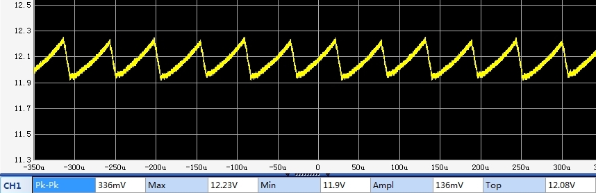
The scope capture below shows a what a typical output ripple looks. In this case, the ripple is 336mV peak-peak riding on a 12VDC output. The frequency is 150kHz which is the operating frequency of the converter IC.
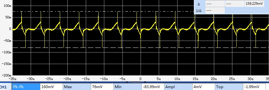
The scope capture below shows the output of a different DC-DC converter which has about 65mV of ripple, but also shows typical noise spikes at the peaks of the waveform that increases the total ripple and noise to about 156mV peak-peak.
While ripple and noise seems concerning especially when it starts getting fairly large, for most digital circuits, it does not cause any issues as digital circuits do a pretty good job of ignoring that type of noise. When working with some analog circuits such as an audio amplifier, or some analog types of sensors that type of noise may become more of a concern. It is possible to add a secondary LC filter circuit to the output of the DC-DC converter if lower ripple and noise is desired.
Converter IC Heat Sinking
The converter ICs are often soldered to the PCB ground plane in order to provide a heat sink for the part especially for the smaller DC-DC converters. Larger DC-DC converters often use TO-220 type package which can be attached to large finned heat sinks and may use cooling fans in larger systems. The heat sinking of this component more than anything else usually determines the maximum current that the module can provide.
Looking at a common part like the LM2596 which is used in many of the smaller inexpensive DC-DC converters where the part is soldered to the board, the recommended minimum heat sink size is to use 2 sq. inches of 2 oz copper and up to 6sq. inches for optimum performance. Most of these boards are not even 2 sq. inches in total size and are often made with thinner 1 oz copper to save cost. It is not surprising that these modules will typically overheat and thermally shutdown when the full rated 3A of current is drawn from the IC.
Heat sinks can be applied to the IC to help with the thermal situation, but these are typically fairly ineffective since the heat sink has to be attached to the plastic body of the device since the metal tab is soldered to the board and heat transfer is not very good even with forced air.
Putting all technical mumble-jumble speak aside, a reasonable validation of the operating conditions of a DC-DC converter is the good old finger test. How hot is the converter IC getting, how hot are the electrolytic capacitors getting and how hot is the inductor getting. These will run warm to pretty toasty under normal conditions. If they are getting to the finger burning stage (90-100°C) things are getting too hot.
For short-term prototyping use, pushing the boundaries is usually not a huge concern. Most will safely shutdown if you push them too hard. If you are testing the boundaries, it is safest to sneak up on them slowly. Some devices with thermal and over-current protection will still fail if they are subjected to a sudden large over-current situation. If you are putting these into long-term use where a failure would be inconvenient, then you are going to want to give them an easier life. As a rule-of-thumb, it is not unusual to need to derate these devices to about half the rated maximum power to keep them in their happy zone for a long life.
Useful Links: