Teensy 4.0 Fully Loaded
$32.95
Adds 10 additional I/O pins to Teensy 4.0
7 in stock
Description
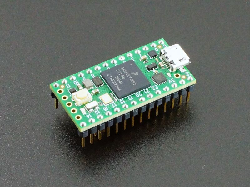
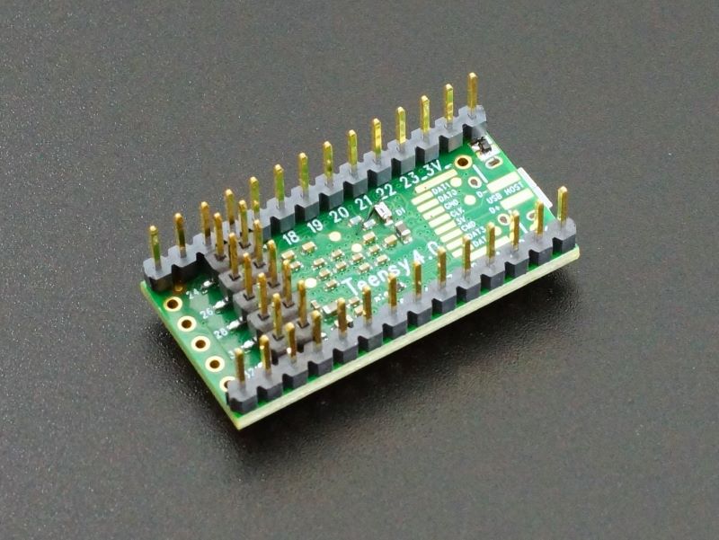
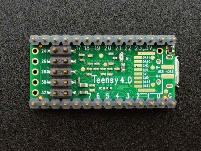
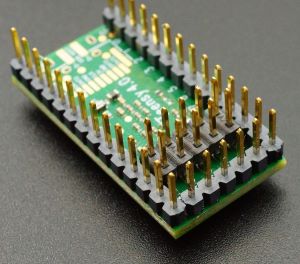
Teensy 4.0 Fully Loaded includes a 10-pin SMD header soldered on the bottom side of the module to provide access to 10 additional I/O pins (D24-D33). In addition, the VUSB/VIN trace is cut and a 1A Schottky diode is added for reverse current protection.
These SMD headers can be a pain to source and tricky to properly align and solder in place, so we are offering a version with these headers preinstalled for those that need this pin arrangement. Since these are typically used with a custom PCB, we also include the VUSB/VIN reverse current protection diode as they are difficult to install after the fact.
In many cases, if more I/O is required than the standard Teensy 4.0 can provide, a move to the Teensy 4.1 will address that issue. In some cases, the very small form factor of the Teensy 4.0 may be required or desired in which case the 10 additional I/O pins on this module may make or break a project.
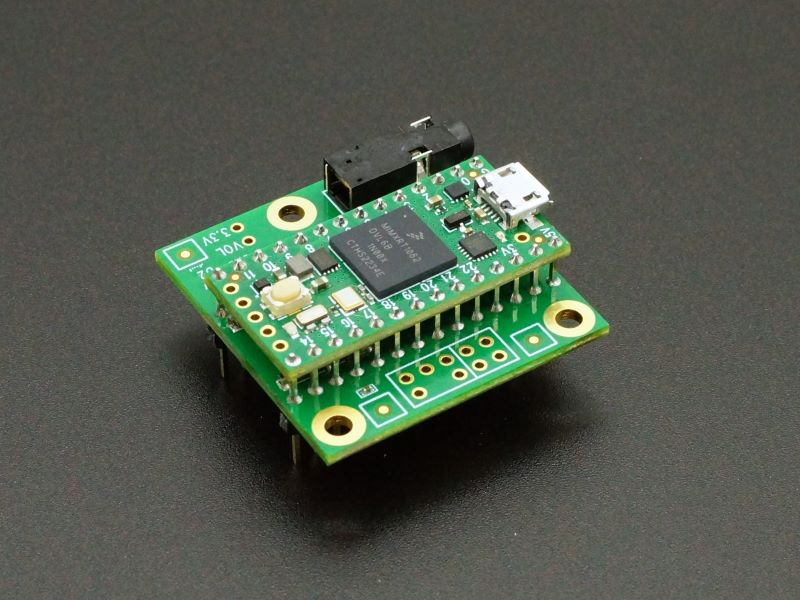
Note: The bottom mounted SMD header prevents this version of Teensy 4.0 from plugging into a standard solderless breadboard. These are typically used with a custom PCB with the necessary sockets to connect to the bottom mounted I/O or a similar setup can be built using standard solder type perf board.
If you are looking for the standard breadboard compatible version or want the full specs for Teensy 4.0, head to this link: https://protosupplies.com/product/teensy-4-0/
Package Includes:
- Teensy 4.0 configured as outlined below
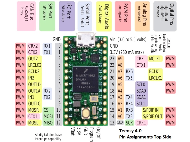
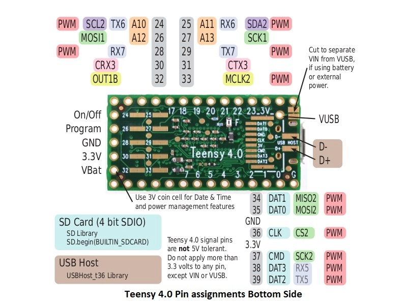
- Handy pinout diagram
The following changes are made to the the base Teensy 4.0 product:
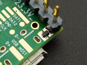
- The VUSB/VIN trace is cut
- An SMD 1A Schottky diode is soldered across the VUSB/VIN pads
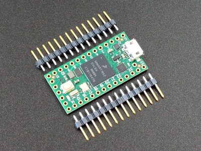
- Standard 1×14 (x2) selectively plated gold headers (pins) are installed
- SMD 2×5 selectively plated gold header is installed on bottom SMD pads
Note: No pins are added to the 2 USB host pads on the bottom of the Teensy. These pads won’t fit a standard 2-pin SMD header and the pads would easily lift off the PCB with any sideways pressure if a header was fitted. Connection to these pads is normally done by using spring-loaded POGO pins on the baseboard that make contact with these pads.
If you need the 1×5 ON/OFF/Program/VBAT header added as well as shown below, add that note to the Order Notes section when you go to checkout and it will be added at no additional cost.
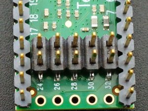
SMD 2 x 5 Header
The SMD header adds 10 additional I/O lines which add a number of different options to the Teensy 4.0.
- 10 digital pins (D24 – D33)
- 4 analog input pins (A10-A13)
- 5 PWM pins
- 2 serial ports (RX6/TX6 – RX7/TX7
- 1 CAN bus (CRX3/CTX3 – CAN 3 which is CANFD compatible)
- 1 I2C bus (I2C2)
- 2 digital audio pins
The pins are physically aligned on standard 0.1″ centers in-line with the D9-D10 and D15-D16 side pins.
The ends of the SMD header pins extend approximately 1mm longer than the side header pins, but this does not create any issues in practice.
VUSB / VIN Diode
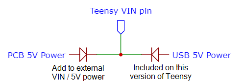
By separating the VUSB and VIN (5V) power inputs and placing a Schottky diode between them, this helps protect the USB connected computer if VIN power is also applied by preventing current from flowing from the VIN 5V source into the device connected to the USB port which will typically be a computer. Since space it very tight, we throw this on in case it is needed and it won’t hurt if it isn’t needed.
For full power protection in a system where both USB and VIN power may be applied at the same time, a 2nd diode should be added to the main VIN (5V) input power. That ensures that current can’t flow in the wrong direction to either the USB connected device or the 5V power source. Though Schottky diodes are typically used, a regular rectifier type diode of 1A or greater can also be used like a 1N4001. A silicon diode will drop more voltage than the Schottky (0.6V vs. 0.3V), but since the Teensy 4.0 is using a 3.3V regulator to drop the 5V down to 3.3V anyway, a little larger voltage drop through the diode doesn’t hurt.
Both diodes should have the cathode (band) facing toward the Teensy VIN / 5V pin as shown here.
Before they are shipped, these modules are:
- VUSB/VIN trace cut and 1A Schottky diode added
- Standard header pins soldered on
- SMD 2×5 male header soldered on
- 5-pin ON/OFF/Program/VBAT header soldered on to bottom of Teensy (if requested by customer)
- Flux cleaned
- Basic functionality reverified by downloading Blink example program
- Packaged in resealable ESD bag for safe storage.
Further Reading:
PJRC Forum – Excellent source of technical information
PJRC website – Good source of information with many example applications in blog posts.
Board Schematics – Scroll down for different schematics.
RT1060 Memory Map – Scroll down toward bottom of page.
Notes:
- None
Technical Specifications
| Microcontroller | NXP iMXRT1060 ARM Cortex-M7 |
| Clock Speed | 600MHz nominal (Optionally 24MHz to 1.008GHz w/ cooling) |
| RAM | 1MB (1024K) |
| FLASH | 2MB (2048K) |
| I/O Logic Levels | 3.3V |
| 5V I/O Compatibility | None |
| Output Pin Drive Current | 10mA |
| DC Current that can be drawn from 3.3V Pin | 250mA maximum |
| Operating Voltage | 3.6 – 5.5V on VIN or VUSB pin |
| Typical Operating Current | 100mA typical @ 600MHz |
| Built-in LED | Attached to digital I/O Pin 13 |
| USB Connector Style | Micro-B Female |
| Board Dimensions (PCB) | 36 x 18mm (1.4 x 0.7″) |
| Country of Origin | USA |
| Mfr | PJRC |
| Datasheet | NXP IMXRT1060 |
| Reference Manual | NXP IMXRT1060 Reference Manual |

