Power MOSFET N-Ch 60V/220A NTP5860NL
$2.95
Handles up to 60V @ 220A, very low Rds(on) of 3mΩ and is logic compatible.
Out of stock
Description
The Power MOSFET N-Channel NTP5860NL is an Enhancement Mode MOSFET that can handle up to 60V @ 220A and is 5V logic compatible.
PACKAGE INCLUDES:
- Power MOSFET N-Channel NTP5860NL
KEY FEATURES OF POWER MOSFET N-CHANNEL NTP5860NL:
- N-Channel Power Enhancement Mode MOSFET
- Up to 60V and 220A power handling capability
- RDS(on) = 3.6mΩ at 4.5Vgs / 3.0mΩ @ 10V
- 5V Logic compatible, partially 3.3V logic compatible
MOSFET stands for Metal Oxide Semiconductor Field Effect Transistor which is why we just call it a MOSFET for short. Enhancement mode means that when the device has zero Gate voltage, the device is off. This is denoted by the schematic symbol with the broken line which indicates that it does not conduct when there is no Gate voltage.
Power MOSFETs are most often used a switches where they are turned fully ON or OFF to control a load such as a motor or high power LEDs. They are ideally suited for this because when the MOSFET is turned fully ON (Saturation Region), it has a very low resistance and can pass a lot of current without much power being dissipated in the device similar to a mechanical switch. When they are turned OFF (Cut-Off Region), they act as an open circuit much like a mechanical switch would when it is off.
For some applications MOSFETs are also used in their Linear Region where they are are partially conducting, such as for an amplifier, analog fan speed controller or battery charger.
The very low ‘ON’ resistance of this device is only 3.6 mOhm at 4.5V gate drive which means that there is very little voltage drop through the device and that also helps to keep power dissipation down.
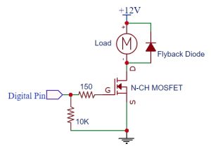
If using this device with a 5V uC, it is possible to drive the MOSFET gate directly from a digital output pin.
The part is also mostly compatible with 3.3V logic. Use of a pull-up resistor on the pin that drives the MOSFET may be beneficial to ensure the full voltage swing.
N-Channel MOSFET Theory of Operation
MOSFET spec sheets can look pretty complicated, but for many applications we just need to pay attention to a few key parameters that are explained here.
VDS : Drain-To-Source Voltage is the maximum voltage that the device can be used to switch. If you’re switching 12V, you need a device with a VDS > 12V and usually you want something with a fair amount of safety margin.
ID : Continuous Drain Current is the maximum current that the device can handle. this will often be specified under several conditions such as at 25C room temperature and at 100C or similar high operating temperature. Achieving the maximum current through the device assumes that you are driving it fully on and that appropriate heat sinking is applied. If you have a device that draws 10A, you need an ID > 10A. Generally the higher the ID rating of the device compared to the amount of current you need to pass though it, the easier it will be to manage thermals.
VGS : Gate Voltage is the voltage differential between the Gate and the Source which is how hard the MOSFET is being driven.
VGS(th) : Gate Threshold Voltage is the voltage at which the MOSFET starts to conduct. Any voltage less than this will drive the MOSFET to the OFF state known as the Cut-Off Region. To possibly be logic compatible, the VGS(th) needs to be well under the logic high voltage level.
RDS(on) : Static Drain-to-Source On-Resistance is the minimum resistance of the MOSFET when it is driven to the fully ON state known as the Saturation Region. The key to look for here is that RDS(on) may be specified at one or a couple of VGS voltages.
If it is spec’d at 10V only, the part is not logic compatible and needs something close to 10V to drive it into saturation. This means a MOSFET driver, transistor or some other means is required to drive the gate with something close to 10V.
If there are two voltages listed, the highest voltage will be the voltage at which the device is fully saturated and show the lowest resistance, often 10V. The lower voltage is often around 4.5V and shows the resistance if you were to drive it directly off of 5V logic. Having this specified implies that the device is at least partially 5V logic compatible even if it isn’t being driven to full saturation.
Looking at the example spec sheet below, this is telling us that to drive the MOSFET to full saturation requires a VGS voltage of 10V where max resistance is 8.7mOhm. If we were to drive it instead at 4.5V directly off of 5V logic, the resistance basically is twice as high, but is still only about 16mOhm.
A device like this can be driven directly off of 5V logic, but because its internal resistance is twice as high, it will drop twice the amount of voltage and dissipate twice as much power/heat in the device for the same current. From a practical standpoint, this means it can handle about 1/2 the full rated current than it could handle if it was driven at 10V. I would consider this as being partially 5V logic compatible. If you are using a 60A device to control a 20A load for instance, this will generally be fine. If you need 40A out of it, then you will need to drive it harder.
Notes:
- None
Technical Specifications
| Maximum Ratings | ||
| VDS | Drain-Source Voltage | 60V |
| ID | Drain Current | 220A |
| RDS(on) | Drain-Source On-Resistance VGS = 10V | 3.0mΩ |
| Drain-Source On-Resistance VGS = 4.5V | 3.6mΩ | |
| PD | Power Dissipation | 283W (requires heat sink) |
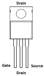
| Package | TO-220 | |
| Package Type | Plastic Tab, 3-lead, through hole | |
| Mfr | ON Semiconductor | |
| Datasheet | NTP5860NL |
Further Reading:
Nick Gammon tutorial on driving motors or other loads with power transistors.


