Hi-Speed SPI Logic Level Converter Module
$2.49 – $3.49
Converts SPI bus Up or Down using SN74LVC2T245 buffers
Select Pins Loose or Pins Soldered
Description
The Hi-Speed SPI Logic Level Converter Module can convert logic levels up or down anywhere from 1.65V to 5.5V at full SPI speeds. Typically used for conversion between 3.3V and 5V devices but can also provide for Vcc isolation between powered and unpowered Master / Slave devices or to improve drive strength.
PACKAGE INCLUDES:
- Hi-Speed SPI Logic Level Converter Module
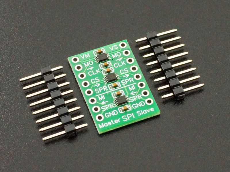
- Qty 2 8-pin male header strips, optionally soldered on
KEY FEATURES OF HI-SPEED SPI LOGIC LEVEL CONVERTER MODULE:
- 4 Master out channels and 2 Master in channels
- Convert logic levels Up or Down
- Converts voltage levels anywhere between 1.65 to 5.5V systems
- Operates over full SPI speed range
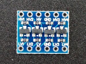
MOSFET Level Converter
The vast majority of logic level shifters on the market utilize MOSFET transistors for the conversion process. These work great for relatively slow speed signals of under 1Mhz, especially when the signals need to be bi-directional such as with I2C. We sell these ourselves. Unfortunately, when these MOSFET modules are used for SPI, their speed limitations often prevent them from working at all, or worse they create intermittent communications that can be hard to diagnose.
This module on the other hand is specifically designed for handling the full range of SPI bus speeds which can be up to 60MHz or even greater by using high-speed buffer ICs. All data lines on the module are routed straight across the module with no vias and the chips have bypass caps on all power pins to optimize performance.
Module Operation
This module is typically used to connect 3.3V and 5V SPI buses together, but it is compatible with a wide range of voltages from 1.65V to 5.5V on both the Master and Slave side for converting either up or down between 1.8V, 2.5V, 3.3V or 5V systems. There are 2 voltage pins on the module. VM is the voltage utilized by the SPI Master device and VS is the voltage used by the SPI Slave device.
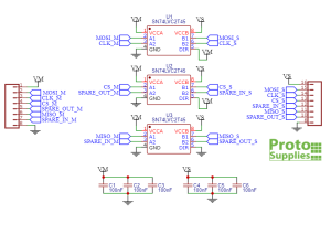
SPI does not require bi-direction capability, but there are both outbound and inbound signal paths. We have created these modules utilizing three SN74LVC2T245 chips that allow for flexible voltage translation at virtually any SPI bus speeds. Two of these chips are configured to provide 4 outbound signal paths from the Master and the other chip is configured to provide 2 inbound signal paths to the Master. Though targeted for SPI, they can be used to translate other logic signals as well as long as the direction of data flow is kept in mind.
There are 4 Master side pins for the out-bound MOSI, CLK, CS and a spare and there are 2 Slave side pins for the inbound MISO and a spare. The Spare pins aren’t needed for the SPI bus per se but can be useful for level shifting related signals such as Data/Command, interrupts or Output Enables.
The devices have high drive capability and can sink/source up to 24mA,. If both VM and VS are run at the same voltage, the device can be used to increase line drive rather than convert logic levels.
Another useful feature is that the module can provide Vcc isolation. If either of the Vcc power inputs (VM / VS) go to ground, the outputs are put into a high impedance state. This prevents either the Master or Slave side from driving their outputs into the inputs of an unpowered device.
Module Connections
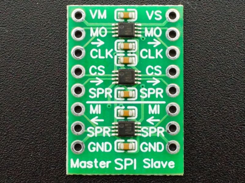
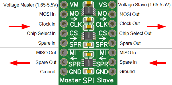
The module is laid out so that the top portion are Master to Slave connections and the bottom portion are Slave to Master connections. The arrows on the module show the direction of data flow. Hookup should be fairly self explanatory.
To use the module, you hook up the two voltages that you want to convert between to the VM (Voltage Master) and VS (Voltage Slave) inputs. These voltages should match the operating voltage of the respective devices.
The GND (ground) connections should be common with the ground of both logic systems. The module has 2 ground pins which are tied together on the module.
The board has the following I/O connections:
- VM = Voltage Master 1.65 – 5.5V
- VS = Voltage Slave 1.65 – 5.5V
- GND = Ground. Should be common to both voltage systems. Only one ground pin needs to be connected
- MO = MOSI from Master to Slave
- CLK = CLOCK from Master to Slave
- CS = CHIP SELECT from Master to Slave
- SPR (top) = Spare from Master to Slave
- MI = MISO from Slave to Master
- SPR (bottom) = Spare from Slave to Master
ASSEMBLING THE MODULE
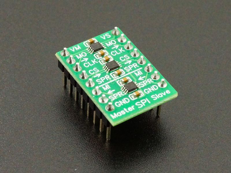
The module comes with 2 strips of straight male headers. These can be soldered on for use with a breadboard, or you can use right-angle headers or attach wires directly to the board depending on what your application requires.
To ensure good alignment during soldering first insert the loose headers into a solderless breadboard. The board can then be placed on top of the headers and easily soldered in place.
The module can also be ordered with these pins already soldered on for plug-n-play operation.
OUR EVALUATION RESULTS:
We created this module because to our knowledge, no similar module exists and many SPI issues are traced to logic level converters that are not well suited for the SPI bus speeds.
The TXS0108E module is often used for SPI level conversion and often work adequately. The issue that sometimes crops up is that these devices are bi-directional with automatic direction detection and that auto detection sometimes runs into problems when pullups are used on the data lines or if connecting to devices that are not push-pull devices. The TXS0108E maximum speed also tends to top out around 20MHz, so are not suitable for fastest SPI speeds.
These modules, by using high-speed logic with fixed predetermined direction flow helps to resolve these issues. The practical maximum operating speed is mainly limited by the wiring used to make the SPI connections, characteristics of solderless breadboard connections as well as the inherent speed capability of the Master/Slave SPI devices involved.
BEFORE THEY ARE SHIPPED, THESE MODULES ARE:
- Sample tested per incoming production build.
Notes:
- None
Technical Specifications
| Operational Ratings | ||
| VM | Voltage Master Side | 1.65V – 5.5V |
| VS | Voltage Slave Side | 1.65V – 5.5V |
| Maximum Chip Data Rates | 420 Mbps (3.3-V to 5-V translation) 210 Mbps (translate to 3.3 V) 140 Mbps (translate to 2.5 V) 75 Mbps (translate to 1.8 V) |
|
| Dimensions | L x W (PCB) | 22.86x 15.72mm (0.9″ x 0.62″) |
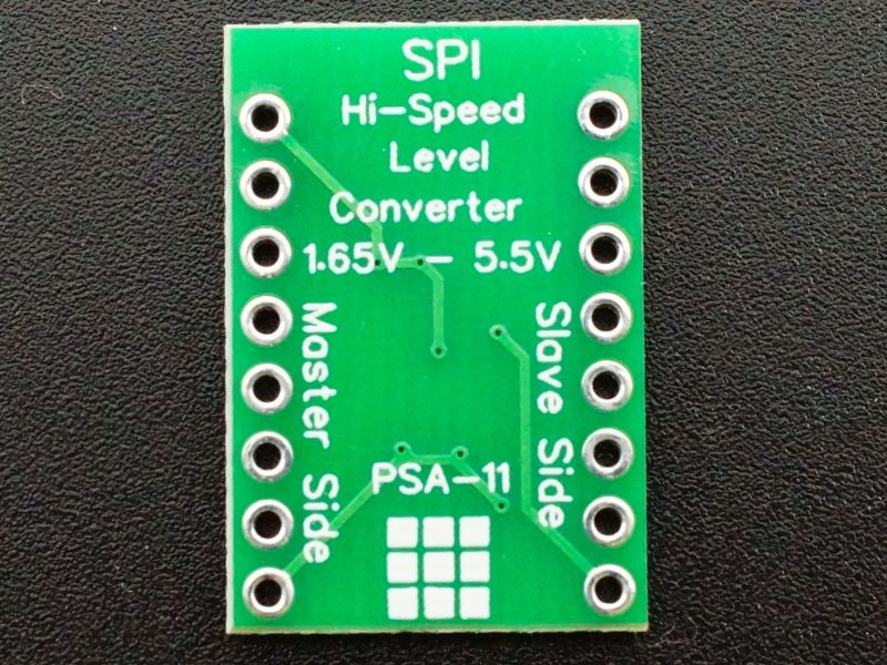
| Footprint | DIP-16 on 0.5″ centers | |
| Country of Origin | Designed in USA | Manufactured in China |
| Datasheet | Texas Instruments | SN74LVC2T45 |
FURTHER READING

